High Density Interconnects Be Repaired
The PCB industry continues to evolve, introducing new products and technologies to cater to the needs of the times. One such product is high density interconnect, which enables the production of smaller PCBs without compromising on performance. The technology makes use of advanced techniques to reduce the size and weight of the circuit boards. It also allows for greater connection pad density and shorter trace lengths.
The technology is used in various electronics and electronic devices, including computers, tablets, laptops, touch screen products, and portable X-ray equipment. It has also been incorporated in wearable technology, including smartwatches and virtual reality headsets. HDI PCBs are able to withstand harsh environmental conditions, making them suitable for military and aerospace applications.
High-density interconnect is a form of PCB technology that involves the use of smaller pads, vias, and spaces, resulting in a lower layer count. This means that the traces on an high density interconnect PCB are shorter, which allows for faster signal transmission and improved device functioning. It also helps reduce power consumption and enhances signal integrity.

Can High Density Interconnects Be Repaired If Damaged?
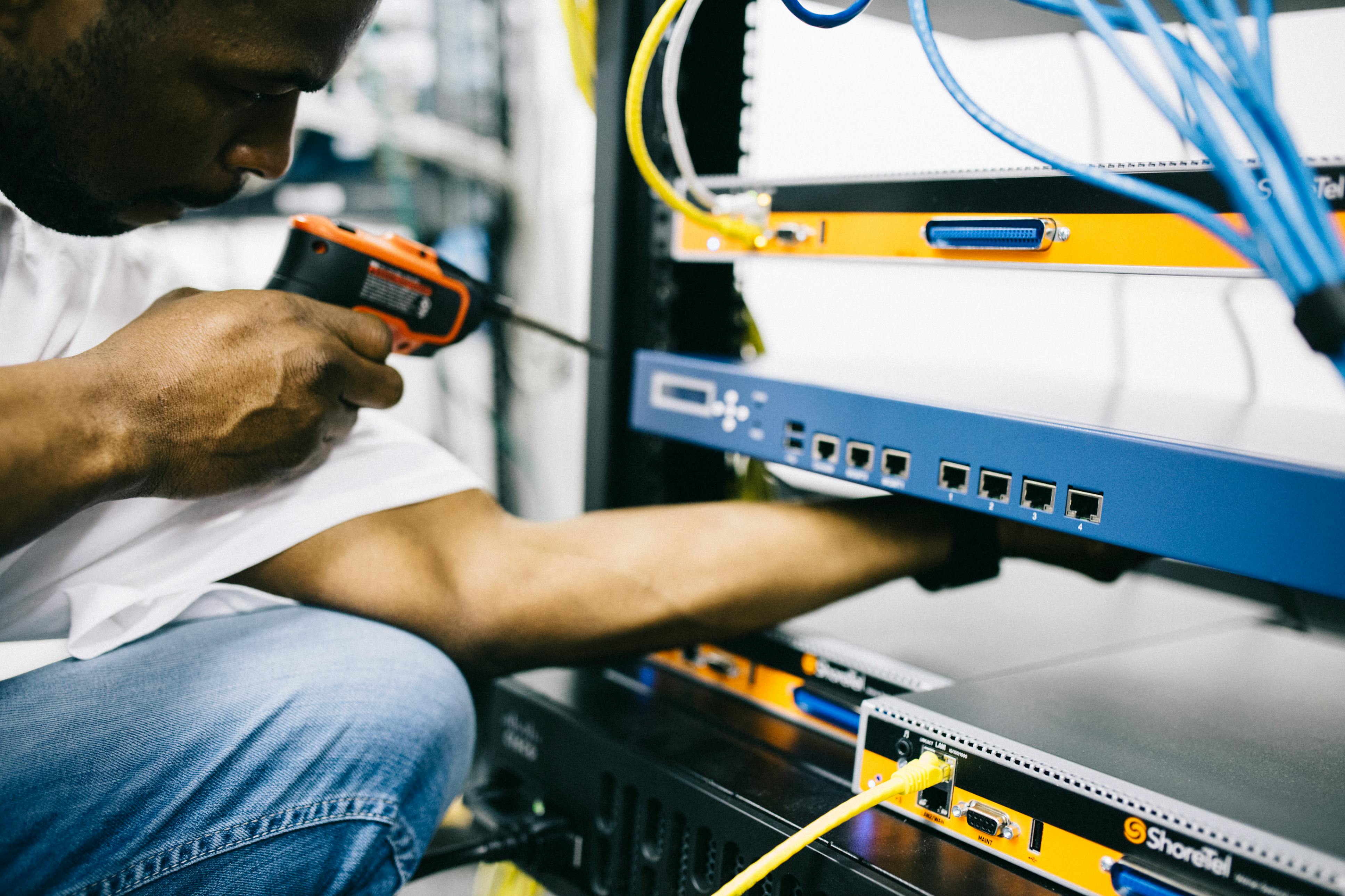
The design and fabrication of a high-density PCB requires complex machinery, which is why it is so important to hire a reputable manufacturer who is experienced in producing this type of circuit board. The process starts with creating a photomask, a template that includes the entire circuit layout. This is then etched into the substrate using innovative photolithography machinery and reactive ion etching. The photomask must be created with precision, as even the slightest deviation can cause significant board failure.
Unlike traditional PCBs, which have through holes to connect outer layers, HDI PCBs use microvias, which are plated on the inner surface of the substrate. These microvias have a diameter of 0.006 mm or less, and they are drilled by either mechanically or laser, depending on the required hole size. The resulting vias are called blind and buried vias, and they can be filled with conductive or non-conductive material.
In addition to microvias, high-density interconnect PCBs also use another technique called via-in-pad, where vias are placed directly under the surface mount component solder pads instead of routing the traces around them. This is a cost-effective method to decrease the thickness of a PCB and improve its reliability, as it reduces the likelihood that solder will wick through the pads and damage the back layer.
Besides these features, high-density interconnect PCBs are capable of supporting smaller components, such as those with higher speed signals. As a result, they are perfect for mobile devices that need to communicate with other devices. This is why high-density interconnect PCBs have become a popular choice for electronic devices, such as cell phones and tablet computers. They are also used in industrial automation, such as manufacturing, warehousing, and inventory management.