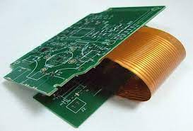
Calculate the Bend Radius for a Flex PCB?
The flex circuit board’s flexibility allows it to be bent and shaped for better design fit. However, there is a limit to the amount of strain that a flex pcb board can sustain. That limit is the bending radius, which is typically ten times the thickness of the circuit board. The bending radius is essential to prevent the copper wires or through holes on the circuit board from breaking due to excessive bending. Moreover, the bending radius is essential to ensuring that the flexible circuit board has the necessary durability for its intended use.
The minimum bending radius for a flex circuit board depends on the type of circuit board material and thickness. It also depends on the conductive trace size and number as well as the cover layer materials. The higher the density of the conductive trace and the cover layer, the more stress is exerted on the board when it is bent. Therefore, the bending radius should be larger to avoid damaging the copper wires and the through holes.
It is important to consider the bending radius during the initial phase of PCB design because it will determine how the circuit board will be used. If the flex circuit board will be used in a dynamic application, then it is likely that it will need to withstand repeated bending. In addition, the bending radius must be sufficient to handle the mechanical stresses of the environment where the flex circuit board will be installed.
How Do You Calculate the Bend Radius for a Flex PCB?
When designing a flex circuit, it is best to choose a symmetrical stack-up of two layers. This will help to reduce the overall cost of production and will also increase the reliability of the circuit. In addition, avoiding 90o bends will reduce the amount of stress placed on the flex circuit. Instead, it is best to use gradual and large curved bends that will not damage the circuit. It is also advisable to stagger the conductors in multi-layered circuits. This will decrease the risk of failure due to fatigue and increased stress that can cause thinning of the copper circuits at the neutral axis during bending.
Moreover, it is crucial to consider whether the circuit board will be manufactured with panel plating or pad-only plating (button plating). While panel plating is cheaper and easier to manufacture, button plating offers more reliability. The reason is that it allows for greater etch yield and copper thickness control for through-holes and pads. In addition, it can also improve conductive performance and eliminate impedance problems in high-speed applications.
Another factor that should be considered when calculating the minimum bending radius is the type of base film that the flex circuit board is made from. Currently, there are several different options to choose from including polyimide, polyethylene naphthalate (PEN), and polyetherimide. It is best to consult with the flex PCB manufacturers about the different options available. They can assist you in selecting the optimal base film thickness for your flex circuit.