Printed Circuit Board Assembly Process
In a printed circuit board and assembly (PCB), conductive pathways engraved within laminated copper sheets are used in combination with non-conductive materials to create an electronic device. To complete a PCB assembly, the soldering and installation of components is required. During this step, the assembly process follows the PCB design blueprint and applies the required components. The process may include both through-hole and surface mount components. To ensure the quality of the final product, assembly operations follow rigorous quality assurance and inspection guidelines.
To prepare for component placement, a computer program creates a profile that specifies how the individual pieces cut from the construction board will be separated. The profiles contain information such as the number of layers, hole sizes, and pitch, which are all relevant for component placement and soldering. Once the profile is ready, the fabrication engineer can use it to guide a machine that cuts the individual boards into smaller pieces. These individual units are then ready for the plating process. The plating process bathes the board in a series of chemicals, which fuse the different layers together. The copper that is deposited during this step also fills in the walls of the holes that were previously drilled.
Prior to the soldering process, a visual and electrical inspection of the PCB takes place. This allows the assembler to identify potential defects and verify that all necessary parts are available for the final assembly. A thorough inventory check is conducted to verify that the correct resistors, capacitors, diodes, transistors, and integrated circuits are present on each of the PCB pieces.
The Printed Circuit Board Assembly Process
Once all of the appropriate components have been verified and are available, the assembly can begin. The first step in the process is referred to as “through-hole” or PTH, and it involves inserting the component leads into pre-drilled holes on one side of the PCB. This is typically the most time-consuming part of the assembly process, but it is essential for the proper functioning of the final product.
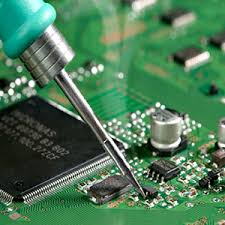
The next step is called SMT or SMD, which refers to surface-mount technology. During this process, automated pick-and-place machines orchestrate the arrangement of each component. Once the component placement is complete, the assemblage is put on a conveyor belt and runs through a specialized oven for soldering. Wave soldering caters to through-hole components, while reflow soldering is for surface-mount devices.
There are many factors that impact the overall cost of a PCB, including labor costs and the specific technology that is employed. The latter factor is an important one, as it demonstrates a manufacturer’s commitment to following industry norms and standards. Adherence to these guidelines not only fosters quality and efficiency, but it also supports ethical business practices. Ultimately, this is beneficial for manufacturers and their customers alike. In this way, the production of a high-quality PCB assembly can be completed in an environmentally responsible manner. This helps to build trust among consumers, suppliers, and regulatory authorities. Achieving this level of integrity is essential for a company’s reputation and long-term success.